FM Transmission and Reception
Pages 130-135
Rider, John. F., and Seymour D. Uslan
John F. Rider Publisher, Inc., 1948.
THE GENERAL ELECTRIC TRANSMITTER
The original f-m transmitters manufactured by the General Electric Company were the direct f-m type employing the regular electronic automatic frequency control system similar to that discussed in connection with the CBS transmitter. The f-m multiplication system in these original transmitters employed two triplers for a total frequency multiplication of 9. In the new f-m transmitters the General Electric Company employs a completely different system. The new system is one of indirect f.m. where p.m. is the initial type of modulation. By using the proper audio frequency correction network the p-m signal is made equivalent to an f-m signal. The method of obtaining the initial amount of phase deviation is new. In these transmitters the famous Phasitron tube is employed as the modulator and the operation of the transmitter is based upon this tube. Before we analyze the complete exciter and modulator system, let us first study the Phasitron tube and see how it works.
The GE Phasitron Tube
The Phasitron tube enables us to obtain wide phase deviations, equivalent to a peak frequency deviation of about 175 cycles, from a crystal controlled source of about 200 kc. The tube itself is quite a complicated structure so far as regular electron tubes are concerned. It more nearly belongs to the class of the cathode-ray tube than to any other type, although its size is comparatively small. A cutaway pictorial view of the Phasitron tube is shown in Fig. 4-13, while Fig. 4-19 provides a more technical cutaway view of the functioning elements together with a simplified diagram of the circuit elements to which it is wired. In Fig. 4-19 all the parts shown are definite physical parts, except the so-called electron disk which is formed by a constant stream of electrons emanating from the cathode and focused on anode No. 1.
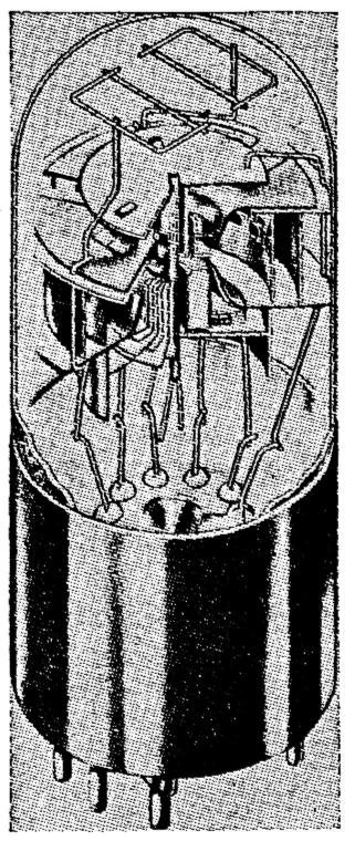
Figure 4-18. Cutaway view of the Phasitron tube, which is used as the modulator and upon which the operation of the GE f-m transmitter is based.
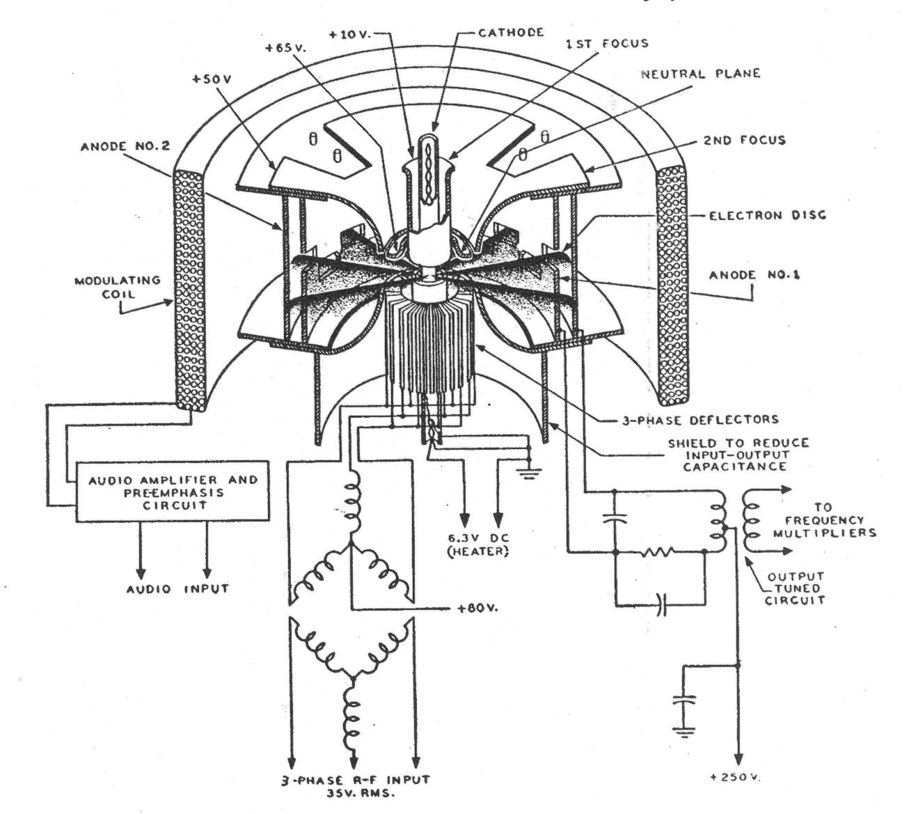
Figure 4-19. Sketch of the functioning elements of the Phasitron tube and a simplified schematic diagram of the circuits to which they are connected. Above and below the electron disk is the deflection system. The deflector grids consist of 36 wires every third one being connected, making three grids each having 12 wires. The voltages indicated in this and the next figure are typical of the slightly different operating conditions.
A schematic diagram of the Phasitron tube is shown in Fig 4-20 with typical operating voltages shown alongside each electrode.
The heater voltage is at 6.3 volts. When typical operating voltages (such as those indicated in Figs. 4-19 or 4-20) are applied to the tube, electrons begin to flow away from the cathode toward the two anodes.
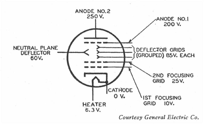
Fig. 4-20. Schematic symbol of the Phasitron tube with typical operating voltages indicated at the various elements.
Without any external r-f voltage applied to the tube, the focusing electrodes regulate the electrons flowing away from the cathode so that they flow in a radial fashion and are concentrated into a thin electron disk, the shape of a flat plate. Above and below this disk is a deflection system. Above the electron disk is the so-called neutral plane of the deflector system, and below the disk are the deflector grids. There are 36 deflector wires, so arranged that every third wire is connected together, making 3 grids with 12 connected wires in each. All the deflector grids and the neutral grid have d-c potentials applied. The deflector grids are, however, excited by an additional r-f voltage while the neutral grid is not. Therefore the neutral deflector (referred to as the neutral plane) remains as a source of reference potential for the other deflector grids. The r-f voltage is a 3-phase voltage obtained from a crystal controlled source. This crystal voltage passes through a phase-splitting network making the r-f voltages applied to each deflector grid group 120' out of phase with each other. For correct operating procedure, the amount of r-f voltage should be approximately 35 volts rms as measured between each deflector grid and the neutral plane deflector. These 3-phase voltages as applied to the deflector grids deflect the electron disk so that the outer edge of the disk takes on a sinusoidal shape as seen in Fig. 4-21. In other words, there now exists an electrostatic field between the neutral deflector plane and the deflector grids, due to the application of these 3-phase voltages. This electrostatic field, due to the deflecting action of the deflector grids, distorts the flat electron disk into the shape shown in Fig. 4-21. The electrostatic field also produces an effect as though the sinusoidal electron disk were rotating at a rate determined by the frequency of the applied 3-phase voltage and the number of deflector wires.
The elements of the Phasitron tube are so arranged that this sinusoidally edged electron disk falls upon the specially constructed anodes of the tube. Both anodes are cylindrical, but anode No. 1 is of special construction. This anode has 24 holes punched into it, so arranged that 12 of these holes appear above and 12 below a certain dividing line. The dividing line is at the level of the electron disk before it is sinusoidally distorted by the application of the 3-phase r-f voltages. Part of this anode appears in Fig. 4-21 in conjunction with the sinusoidally distorted electron disk. A flattened portion of this first anode is also shown in Fig. 4-22. The punched holes are arranged to be in line with the sinusoidal rim of the electron disk.
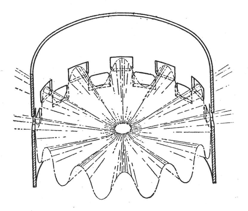
Fig. 4-21. A portion of the Phasitron perforated No. 1 anode through which the sinusoidally distorted electron disk flows; under this condition No. 2 anode receives a maximum current.
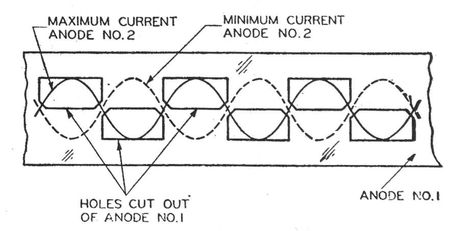
Fig. 4-22. The solid sine wave indicates the condition shown in Fig. 4-21. The dotted wave shows the electron disk one-half an r-f cycle later when a minimum current flows in the No. 2 anode.
Anode No. 1 is nearer the cathode and anode No. 2, which is a cylindrical electrode without any holes punched in it, lies directly behind anode No. 1, as illustrated in Fig. 4-19.
When r-f 3-phase voltages are applied to the deflector grids, the electron disk will become distorted, and the edge of the disk will take on a sinusoidal shape. Let us now refer to Fig. 4-22. This diagram shows by the solid line sine wave a picture of part of anode No. 1 at the instant when the rotating disk is aligned to anode No. 1 so that the upper halves of the sine wave part of the disk are passing through the top 12 holes of the anode, and the lower halves of the sine wave pass through the bottom 12 holes of the anode. Under this circumstance these electrons forming the electron disk are practically all passing through the holes of the first anode and, therefore, hitting the second anode directly in back of it. Consequently, at such an instant there is maximum current flow to anode No. 2 and a minimum current flow to anode No. 1. If the electron disk is rotated by just one-half cycle of the sine wave, the situation will be completely reversed. This is also shown in Fig. 4-22, where the dotted sine wave represents the edge of the electron disk one-half cycle of r.f. later. It is readily seen that the electrons forming the disk no longer pass through the holes in anode No. 1 but that most of them impinge upon anode No. 1 and a very few reach anode No. 2. Under this circumstance, the current flowing to anode No. 1 is a maximum and that flowing to anode No. 2 is a minimum.
For the time between these two instances the current in one anode is decreasing while that in the other is increasing, and after they have reached their maximum decrease and increase, the situation reverses itself. The current that was decreasing in one anode now starts to increase and that which was increasing now starts to decrease.
Connected to the anode of the Phasitron is a push-pull tuned circuit as shown in Fig. 4-19. The circuit is tuned to the crystal frequency and, since each end of the circuit is connected to an anode, this circuit is excited by the periodic collection of electrons by both anodes. Thus it is seen that the output push-pull circuit connected to the anodes is driven at the crystal frequency but, due to the currents of the anodes, the excitation is in a special time and phase relationship. Inductively coupled to this push-pull circuit is a single tuned circuit which serves as the input circuit for the first multiplier tube, and hence the multipliers get their excitation from this coupling arrangement.
Now we come to the important part wherein the phase modulation is produced by an audio signal. Wrapped around the outside of the glass envelope of the Phasitron is the modulator coil which is solenoid wound. Part of this coil is seen in cutaway view (without the glass envelope of the Phasitron tube shown) in Fig. 4-19. This modulator coil, by means of electromagnetic deflection, phase modulates the electron disk. With the proper input audio signal applied to the modulator coil, a magnetic field is set up by this coil, and the coil is so arranged that the magnetic field is perpendicular to the plane of the electron disk. Due to this magnetic field, the electrons encounter a force such that the sinusoidal ripples of the disk experience a phase shift in direct accordance with the audio modulating signal. In other words, the modulating signal, since it varies at an audio rate, shifts the phase of the sine wave edge of the electron disk in an increasing and decreasing motion according to positive and negative portions of the audio signal. The magnetic field created by the coil is concentrated, because of the magnetic material of which the second focusing electrode is made, to a narrow portion of the tube at the rim of the deflector grids; proper phase shift action upon the electron disk is then produced within the punched hole regions of the first anode, as seen in. Fig. 4-23. Thus, this second focusing electrode serves two purposes - electrostatic focusing of the electron disk and electro-magnetic focusing of the audio magnetic field.
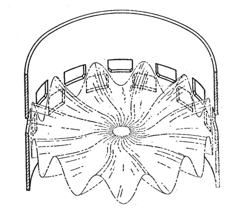
Fig. 4-23. Pictorial representation of the Phasitron electron disk while being phase shifted by the magnetic field set up by the modulating coil.
Since the electron disk is now being changed in phase, according to the audio magnetic field, the output signal of oscillator frequency from the Phasitron, which is coupled to the multipliers, is also changed in phase according to the audio signal. Thus, we have a system of. directly phase modulating a high frequency signal. In order to have the output signal from the Phasitron effectively frequency modulated, the impedance of the modulating coil is practically a pure reactance over the complete range of audio frequencies of 50 to 15,000 cycles. As the audio frequency increases, the reactance also increases, in which case the current flowing through the coil decreases. Therefore, as the audio frequency increases, the magnetic field decreases, due to the decrease in current, thus giving the desired inverse frequency effect. This is similar to the effect of the audio frequency correction network in the Armstrong transmitter, wherein an inverse audio frequency network was needed effectively to produce f.m. from p.m.
Consequently, with all of these provisions, the modulation of the Phasitron tube by the audio signal has the effect of speeding up and slowing down the rotation of the electron disk: along its edge (as shown in Fig. 4-23) which results in an f-m output signal. The importance of this Phasitron tube is that it can produce wide phase shifts in the crystal frequency and, with the proper modulation arrangement, these phase shifts are equivalent, to an f-m signal that has peak deviations as high as 175 cycles. Due to this wide deviation only a small amount of multiplication is needed as compared with other indirect f-m systems. The amount of phase shift required for this 175-cycle peak frequency deviation does not go beyond the allowable amount of harmonic distortion. The audio frequency harmonic distortion for all frequencies from 50 to 15,000 cycles is less than 1.5 percent rms.
Exciter and Multiplier Units
A block diagram of the exciter unit of the GE transmitter is shown in Fig. 4-24. This part of the system comprises the a-f, r-f, and modulator units. It essentially consists of a crystal oscillator and an r-f amplifier feeding into the 3-phase network input to the Phasitron tube.
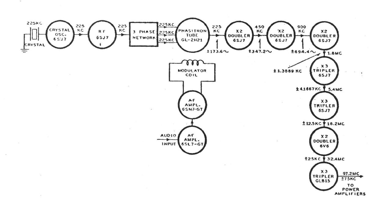
Fig. 4-24. Block diagram of the General Electric f-m transmitter; the power amplifiers are omitted.
Also the audio input is passed through two a-f amplifiers before it is impressed across the modulator coil. The output of the Phasitron tube, being an f-m signal, is fed to a series of seven multipliers having a total multiplication equal to 432. The first three multipliers are doublers using 6SJ7 receiving type tubes, and hence a multiplication of 2 X 2 X 2 or 8 is obtained. The next two multipliers are triplers, also employing 6SJ7 tubes, and their multiplication is 3 X 3 or 9; from the input to the first 6SJ7 doubler to the output of the last 6SJ7 tripler the total multiplication is 8 X 9 or 72. The last two multipliers are a doubler and a tripler, respectively, making a multiplication of 2 X 3 or 6 and a total over-all multiplication of 72 X 6 or 432. The last multiplier (a tripler) employs a GL815 tube which, besides being a multiplier, is also the driver for the power amplifier stage succeeding it. The next to the last multiplier, a doubler, uses a 6V6 tube to supply the small amount of power needed to drive the GL815 tripler tube.
For 100 percent modulation, the output f-m signal must have a peak deviation of 75 kc. This means the necessary amount o-f f.m. that occurs within the Phasitron tube has to be exactly equal to the maximum allowable peak frequency deviation divided by the total amount of multiplication. Thus 75 kc/432 equals 173.6 cycles, which means that the output peak frequency deviation from the Phasitron tube is equal to 173.6 cycles. The individual multiplication of this frequency deviation is illustrated in plus and minus signs next to the particular stages.
If an output f-m signal of 97.2-mc carrier frequency is desired to be transmitted, the frequency of the crystal oscillator would have to be equal to 97.2 mc/432 or exactly 225 kc. This is indicated in Fig. 4-24 along with the respective increase in frequency as the signal is passed through the different multiplication stages. Since the new f-m band is between 88 and 108 mc, the crystal frequency has to be between 88 mc/432, or 203.7 kc, and 108 mc/432, or 250 kc.
A schematic diagram of the crystal oscillator and Phasitron circuit is shown in Fig. 4-25. The crystal oscillator is of the Colpitts electron coupled type wherein the cathode, control grid, and screen grid act as the crystal oscillator section of the 6SJ7 tube.
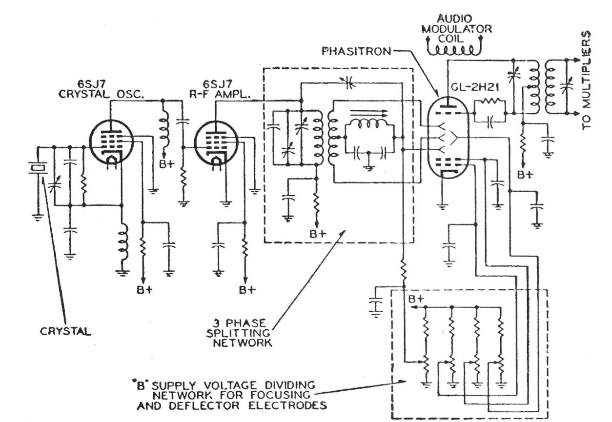
Fig 4-25. Crystal oscillator and Phasitron circuits of the General Electric f-m transmitter.
In this instance, the screen grid serves as the oscillator anode, and the electron coupling occurs between this anode and the plate of the 6SJ7 tube. The output of the second 6SJ7, an r-f amplifier, is tuned-transformer coupled to a 3-phase-splitting network shown enclosed in the dotted box. The output from this phase-splitting network is applied to the three deflector grids of the Phasitron tube. The deflector grids, neutral plane deflector, and focusing electrodes all receive their B supply through a special voltage divider network consisting of four fixed resistors and four potentiometers. These potentiometers are preset so that the correct amount of B supply voltage is applied to these Phasitron electrodes for the proper operation of the tube.